A device that lets a small electrical signal control a large one, with no moving parts, made from a crystal. It replaced the vacuum tube, made computing possible at scale, and is manufactured today in numbers that have no useful comparison.
A transistor is a switch or an amplifier with no mechanism. A voltage or current at one terminal controls the current flowing between two others.
That single property is sufficient for everything electronic. Amplification builds radios and audio. Switching builds logic gates, and logic gates build processors and memory. A modern computer is transistors arranged into gates and nothing else of consequence.
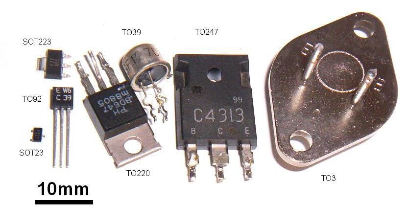
Semiconductors are the key material: substances like silicon whose conductivity sits between conductors and insulators and, crucially, can be controlled.
Pure silicon conducts poorly. Doping it with small quantities of other elements changes that. Adding an element with an extra outer electron produces n-type material with mobile negative carriers; adding one with a shortage produces p-type material with mobile positive vacancies.
Where n-type and p-type meet, a junction forms with a region depleted of carriers, and this junction conducts in one direction and not the other. A transistor is two such junctions arranged so that the middle region controls the flow through both.
The physics required is quantum mechanics: band theory explains why some materials conduct and others do not, and why doping works. The transistor is the first major technology that could not have been designed without quantum theory, which is a useful answer to the question of what quantum mechanics is for.
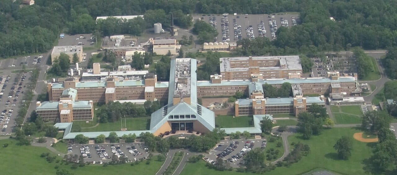
John Bardeen and Walter Brattain demonstrated the first working transistor at Bell Laboratories on 23 December 1947, a point-contact device using two gold contacts pressed onto germanium. It worked and was almost unmanufacturable.
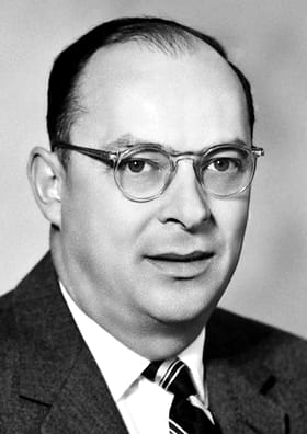
William Shockley, who led the group and had been absent for the demonstration, developed the junction transistor over the following two years. It was a sandwich of doped layers rather than a mechanical contact, it was robust, and it could be manufactured.
The three shared the 1956 Nobel Prize in Physics. Bardeen won a second in 1972 for the theory of superconductivity, and remains the only person to have received the physics prize twice.
Shockley left to found his own company in what became Silicon Valley, and managed his staff so badly that eight of them left in 1957 to found Fairchild Semiconductor. Intel and AMD descend from that departure, so a substantial part of the modern industry traces to one man's failure as a manager.
The integrated circuit, developed independently by Jack Kilby at Texas Instruments in 1958 and Robert Noyce at Fairchild in 1959, put many transistors on one piece of silicon and connected them there. This removed the wiring, which had become the limiting cost.
Gordon Moore observed in 1965 that the number of components per chip had been doubling roughly annually, and predicted the trend would continue. It did, at a rate closer to two years, for half a century. This was not a law of nature but a target the industry organised itself around, which is part of why it held so long.
The numbers are difficult to convey. A first-generation integrated circuit held a handful of transistors. A current processor holds tens of billions. Individual transistor features are now measured in single-digit nanometres, spanning a few dozen atoms. The industry manufactures on the order of a trillion transistors per second, which is more objects per year than any other artefact humans have made by many orders of magnitude.
Conventional scaling is ending, for physical reasons rather than economic ones.
Gate oxides a few atoms thick leak by quantum tunnelling, which wastes power and generates heat that cannot be removed. Power density, not transistor count, has been the binding constraint since around 2005, which is why clock speeds stopped rising and processors gained multiple cores instead.
Manufacturing cost per transistor, which fell for decades, has flattened. Extreme ultraviolet lithography, required below about seven nanometres, is made by a single company and costs upwards of a hundred and fifty million dollars per machine.
The responses are architectural rather than dimensional: three-dimensional stacking, specialised accelerators for particular workloads, and chiplets assembled into packages rather than built as one die.
The one genuinely dimensional response has now shipped. Gate-all-around transistors, in which the gate wraps the channel on every side instead of three, entered volume manufacturing at TSMC's two nanometre node in late 2025 and ramped through 2026. The gain is roughly ten to fifteen percent more performance at the same power, or twenty five to thirty percent less power at the same performance, with logic density up about a fifth. That is a real improvement and it is not the doubling the old cadence delivered.
Node names should not be read as measurements. Two nanometre describes no physical feature of the device; it is a marketing label for a generation, and actual gate lengths are several times larger. Alternatives including carbon nanotube and two-dimensional material transistors remain in research.
The transistor itself is not being replaced. What is ending is the assumption that the next one will be smaller, cheaper and faster than the last, which held for fifty years and shaped every industry that depends on it.