Doping is the deliberate introduction of impurities into a semiconductor in order to control its electrical behaviour. Every transistor, and therefore every computer, depends on it. The quantities involved are astonishingly small, and the fact that such small quantities matter so much is the whole point.
Pure silicon has four outer electrons per atom, each shared with a neighbour, which leaves few carriers free to move and makes it a poor conductor.
Adding an element with five outer electrons, such as phosphorus or arsenic, leaves one electron surplus to the bonding and free to move. The result is n-type material, carrying negative charge. Adding an element with three, such as boron, leaves a vacancy that behaves as a mobile positive charge, called a hole. The result is p-type.
Neither material is charged overall; what changes is which carrier dominates and how many there are. Concentrations are typically in the range of one dopant atom per million to per hundred million silicon atoms, and that is enough to change conductivity by many orders of magnitude.
Doping alone would only make a better resistor. The device physics comes from putting p-type and n-type material together. At the junction, carriers diffuse across and leave behind a depletion region with a built-in electric field, and that field makes current flow readily in one direction and barely at all in the other. That is a diode.
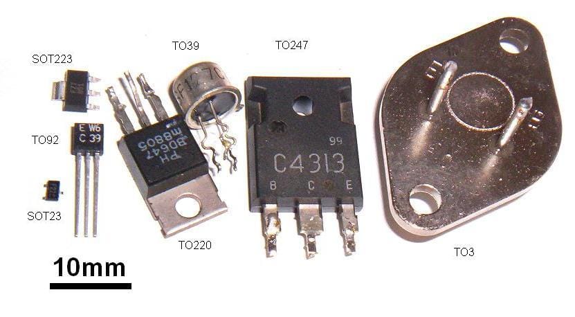
Adding a third region and a control terminal gives a transistor, which can switch or amplify. Because the control is electrical rather than mechanical, it can be made small and fast, and it is this that made the integrated circuit possible: a modern processor contains billions of such structures patterned into a single crystal.
Early doping was done by diffusion, heating the wafer in a dopant-rich atmosphere so atoms migrate in. The dominant modern method is ion implantation, in which dopant ions are accelerated and fired into the wafer, which gives precise control of both dose and depth but damages the crystal lattice, so the wafer is annealed afterwards to repair it and to move dopant atoms onto proper lattice sites. Patterning is achieved by masking, which is what allows different regions of one chip to be doped differently.

Scaling has run into physics. At the smallest dimensions the number of dopant atoms in a transistor channel becomes small enough that statistical variation between nominally identical devices matters, a problem called random dopant fluctuation. Dopants also diffuse during subsequent heating steps, blurring boundaries that need to stay sharp. These constraints are among the reasons the industry moved to three-dimensional structures such as FinFET and gate-all-around designs, which control the channel by geometry rather than relying on doping alone.